PCBA Routing
Efficient PCB assembly routing for controlled, traceable production flow.
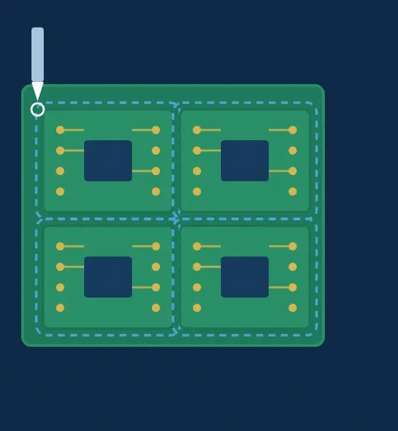
Precision PCB Depaneling for Assembled Circuit Boards
PCBA routing is a PCB depaneling technique used to separate individual printed circuit board assemblies from a shared manufacturing panel. This process is particularly useful when electronic boards have custom outlines, curved edges, or layouts that require controlled separation.
During PCB routing, a cutting tool follows a predefined path around the board profile. The process must account for board dimensions, component placement, panel design, and mechanical tolerances to help prevent damage during separation.
For electronics manufacturers, selecting an appropriate PCB separation method is an important consideration in maintaining assembly quality and preparing circuit boards for subsequent production stages.
PCB Routing Process
The PCB routing process typically involves preparing the panel, configuring the cutting path, separating individual assemblies, and inspecting the finished boards.
1. PCB Panel Preparation
The assembled PCB panel is positioned securely to support accurate separation and consistent processing.
2. Routing Path Configuration
The cutting path is established according to the PCB outline, panel layout, and specified dimensions.
3. Controlled Board Separation
A suitable routing tool follows the programmed profile to separate individual printed circuit board assemblies from the panel.
4. PCB Edge Inspection
The separated boards are checked for dimensional conformity, edge condition, and visible signs of mechanical damage.
5. Post-Routing Handling
Individual PCB assemblies are prepared for the next manufacturing operation, inspection stage, or packaging process.
Benefits of PCBA Routing
- Complex PCB Profiles: Suitable for boards with curved outlines and customized shapes.
- Controlled Separation: Supports accurate cutting along predefined board profiles.
- Component Protection: Appropriate process settings help limit mechanical stress on populated circuit boards.
- Consistent Board Dimensions: Helps maintain the required outline of individual assemblies.
- Manufacturing Flexibility: Can accommodate different panel layouts and PCB configurations, subject to equipment capabilities.
Applications of PCB Depaneling
PCB routing may be used for assembled circuit boards in automotive electronics, industrial control equipment, electronic modules, and other products requiring individual boards to be separated from manufacturing panels.
The appropriate depaneling method depends on PCB thickness, board geometry, component clearance, panel construction, and production requirements.
Choosing the Right PCB Routing Method
Successful PCBA routing requires consideration of the board design and the sensitivity of mounted components. Tool selection, cutting parameters, fixture design, and inspection procedures all influence the final result.
For manufacturers working with custom-shaped or populated printed circuit boards, PCB routing can provide a suitable approach to panel separation when the process is matched to the assembly design.
Tell us the job. Get a quote.
Describe the part, material, quantity and target date. Our engineers reply within one working day.
Other divisions
Popular searches
One-piece Fittings | Two-Piece Fittings | Hydraulic Products | Hydraulic Hose Assembly