Electronics Manufacturing Services (EMS)
High-quality EMS and surface-mount (SMT) assembly, with injection moulding under the same roof.
Polyfit: Your Partner in Comprehensive Electronics Manufacturing Services (EMS) and Surface Mount Technology (SMT) solutions
Polyfit is an A‑Level SQ‑certified company offering state‑of‑the‑art Electronics Manufacturing Services (EMS) under a controlled Class 10K (ISO 7) cleanroom environment. Our advanced facilities are designed to meet the growing demand for high‑precision Surface‑Mount Technology (SMT) assembly, through‑hole soldering, and comprehensive electronic product manufacturing.
Polyfit is a A-Level SQ Certified Company





Injection Moulding
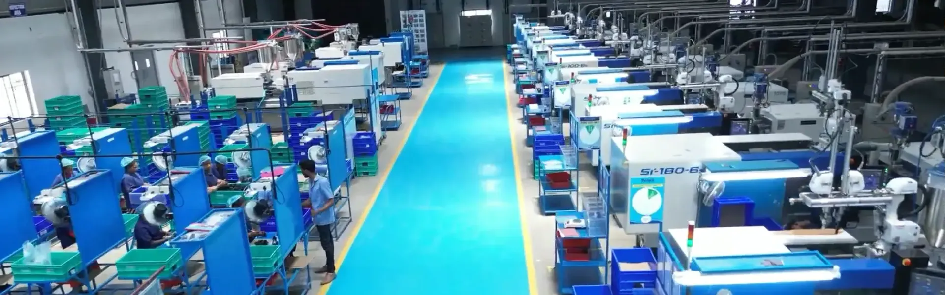
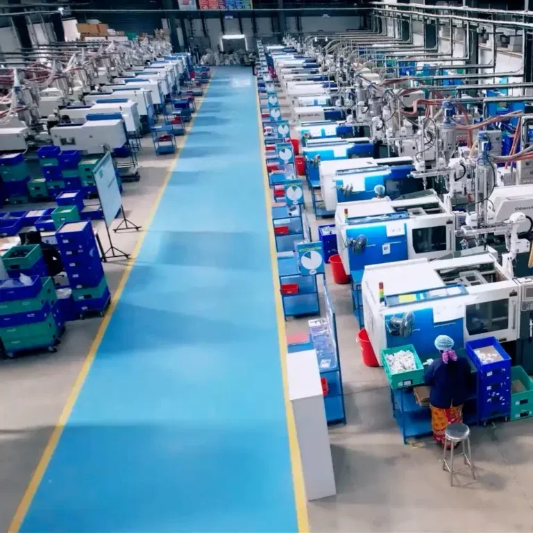
Polyfit offers advanced injection moulding solutions for a wide range of product sizes and complexities.
Our capabilities include:
- Horizontal, vertical, two-platen, twin-color, and all-electric machines
- Fully automated robotics for consistent, efficient production
- AI-powered vision systems for real-time defect detection
- Centralized raw material feeding with auto-dehumidifiers for optimal quality
Our streamlined shop floor features calibrated auxiliary systems, tonnage-specific cranes, and SMED practices for fast, efficient tool changes.
Pad Printing
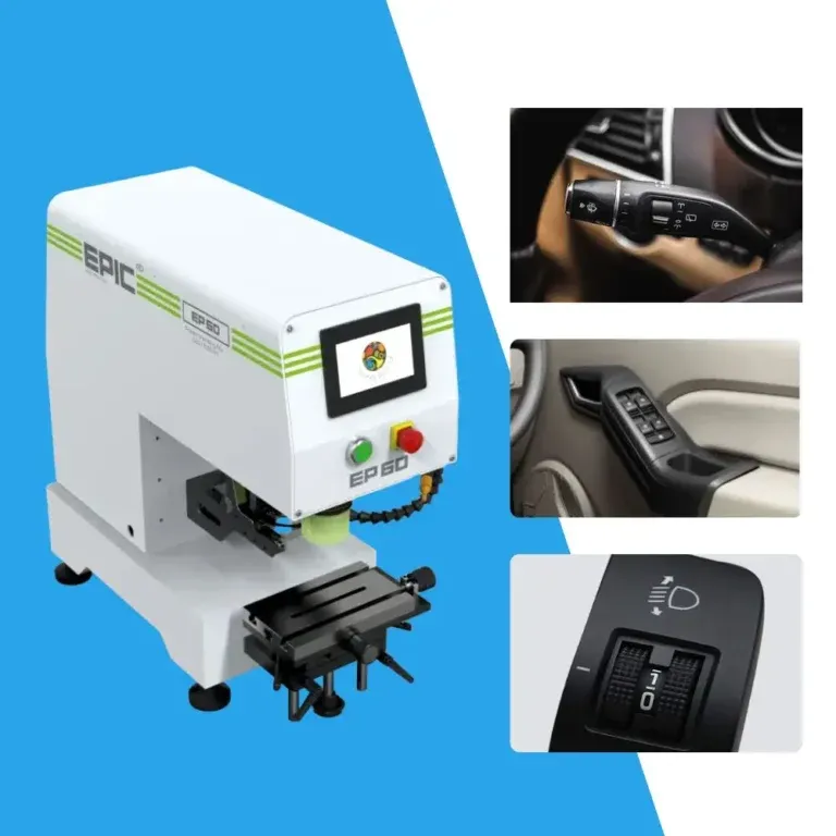
Pad printing is an efficient method for transferring 2D images onto 3D automotive parts, including curved and irregular surfaces. It delivers sharp detail, vibrant color, and strong adhesion using specialized inks suited to various materials.
A soft silicone pad adapts to complex shapes for precise image transfer. This process is ideal for branding, markings, and customization.
High-performance pad printing machines ensure consistent quality, excellent registration, and durability—making them essential for demanding automotive applications.
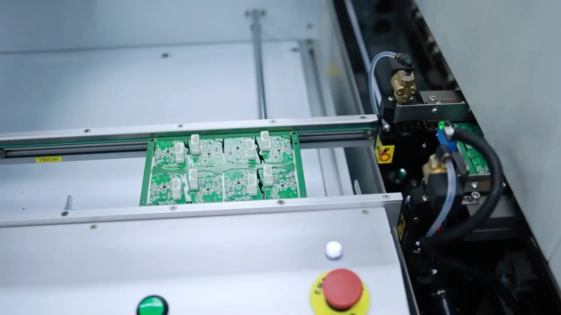
PCB Assembly & SMT Solutions
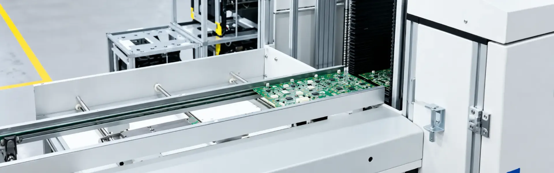
Surface‑Mount Technology (SMT) involves mounting electronic components directly onto printed circuit boards (PCBs) with exceptional precision.
At Polyfit, our Class 7K cleanroom houses a fully automated SMT production line featuring high‑speed pick‑and‑place machines capable of placing up to 90,000 components per hour. Our process includes solder‑paste inspection (SPI), automated‑optical inspection (AOI), and an auto‑rejection conveyor system to ensure continuous, uncompromised quality control throughout the production cycle.

Conformal Coating
Printed Circuit Boards (PCBs) may be exposed to moisture, dust, chemicals, temperature variations, and other environmental conditions during operation. Over time, these factors can affect electronic components, electrical connections, and overall circuit performance.
Conformal coating adds a thin protective layer over the assembled PCB, helping reduce exposure to environmental contaminants and supporting reliable operation. Selecting a suitable coating depends on the circuit board design, component requirements, and the conditions in which the product will be used.
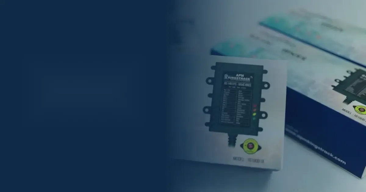
Box Build Assembly Services
Box build assembly is the process of bringing electronic, electrical, and mechanical components together to create a complete product. Depending on the design, this process may involve PCB installation, cable routing, wiring connections, enclosure fitting, and the integration of various components into a finished assembly.
Our approach to box build assembly focuses on following product specifications, maintaining organized assembly processes, and meeting application-specific requirements. From individual electronic modules to integrated product assemblies, the scope of work depends on the design and manufacturing needs of each project.
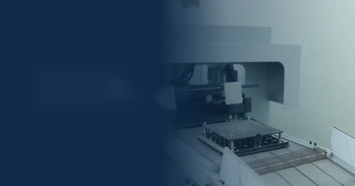
Wave Soldering Services
Wave soldering is a widely used process in electronics manufacturing for soldering through-hole components onto printed circuit boards (PCBs). During this process, the PCB passes over a controlled wave of molten solder, creating electrical and mechanical connections between component leads and the circuit board.
This soldering method supports efficient assembly of electronic products where through-hole components are required. The process parameters are selected according to PCB design, component specifications, and soldering requirements to help achieve consistent connection quality.
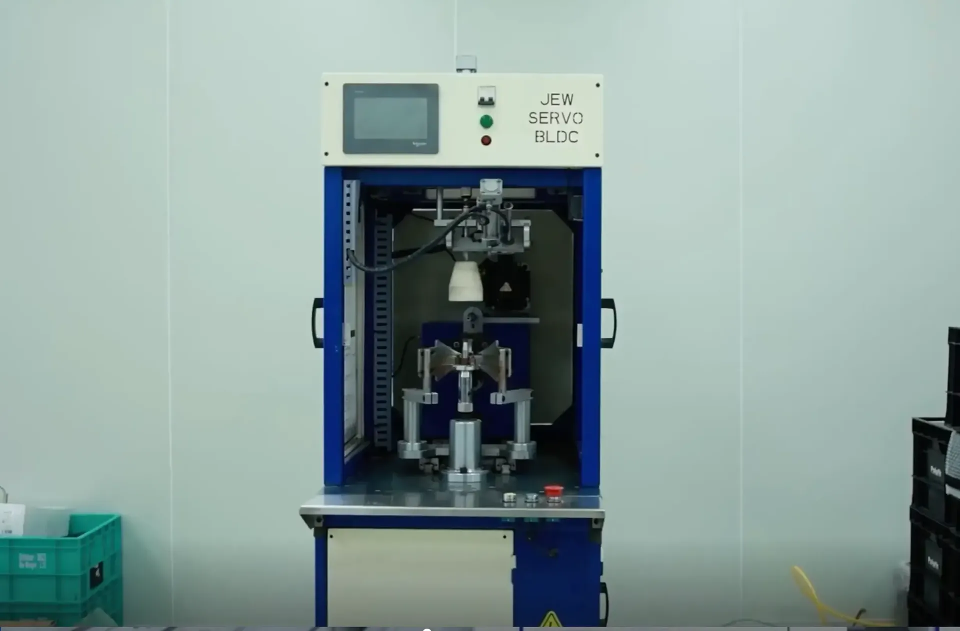
In-Circuit Testing (ICT) for PCB Assembly
In-Circuit Testing (ICT) is a testing method used in electronics manufacturing to examine individual components and electrical connections on a printed circuit board (PCB). It helps identify assembly-related faults before the board moves to the next stage of production.
Depending on the PCB design and test setup, ICT equipment uses probes to access designated test points and measure electrical characteristics. The results are evaluated against predefined test limits to identify potential component or connection problems.
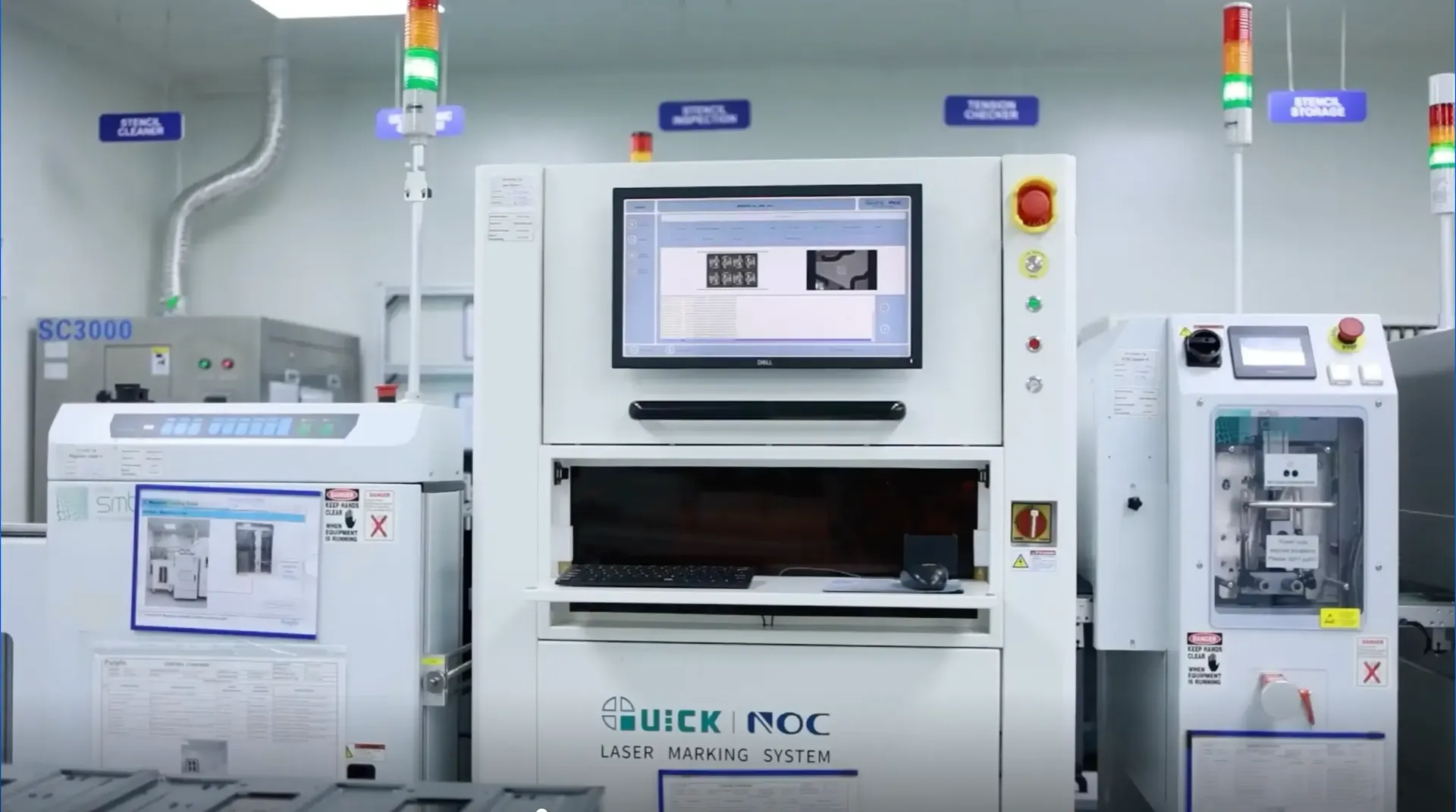
Laser Marking for Traceability
Laser marking is a process used to create identification marks directly on suitable components, materials, and product surfaces. In electronics manufacturing, it can be used to mark printed circuit boards (PCBs), enclosures, and other compatible parts with information such as serial numbers, product codes, batch details, and machine-readable codes.
These markings help identify individual products and support tracking throughout manufacturing and subsequent handling. Depending on the application and material, laser marking can provide clear, durable identification without the need for printed labels.
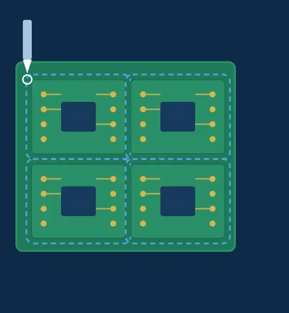
PCBA Routing Services for Electronic Manufacturing
PCBA routing is a PCB depaneling technique used to separate individual printed circuit board assemblies from a shared manufacturing panel. This process is particularly useful when electronic boards have custom outlines, curved edges, or layouts that require controlled separation.
During PCB routing, a cutting tool follows a predefined path around the board profile. The process must account for board dimensions, component placement, panel design, and mechanical tolerances to help prevent damage during separation.
Our Services
Why choose us?
Comprehensive EMS Support
We offer a complete range of EMS solutions, including PCB assembly, functional testing, conformal coating, box build, and supply‑chain management. Our systems are compliant with Moisture Sensitivity Level (MSL) handling standards, ensuring the safe storage and processing of sensitive components. We turn your ideas into reality — supporting every stage of product development and manufacturing, from concept design to mass production and delivery.
World-Class Electronics Manufacturing Services Across All Industries
Polyfit provides world‑class EMS solutions to a diverse range of industries, including automotive, medical devices, industrial automation, consumer electronics, energy systems, and defense electronics.
 Automotive
 Medical Sector
 Charging Station
 Telematics
 Defense
 Electric vehicle
 Telecom
 Power Sector
Tell us the job. Get a quote.
Describe the part, material, quantity and target date. Our engineers reply within one working day.
Other divisions
Popular searches
One-piece Fittings | Two-Piece Fittings | Hydraulic Products | Hydraulic Hose Assembly