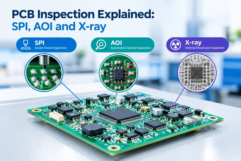
The PCB Assembly Process, Explained Step by Step
Paste, placement, reflow, inspection and test: what happens to a circuit board at each stage of assembly, and where problems get caught.
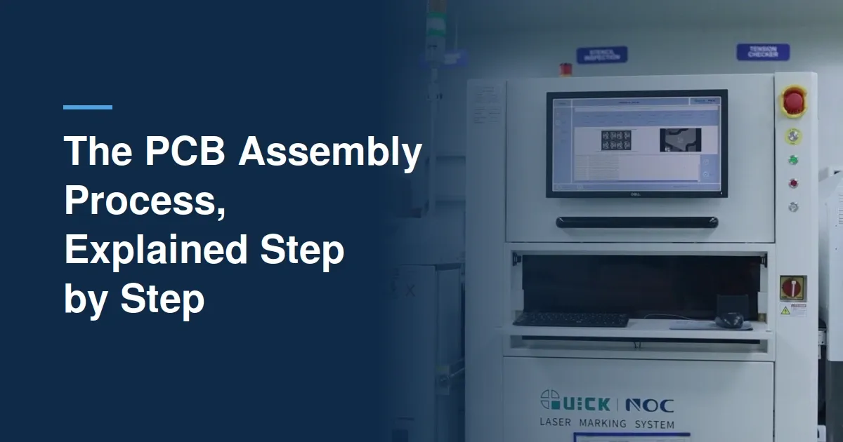
If you have only ever seen a finished board, PCB assembly can look like a black box: bare boards and reels of parts go in, working electronics come out. In reality it is a fixed sequence of steps, and each one has a check built in so that a fault is caught at the stage where it is cheapest to fix.
Here is the sequence a typical surface-mount board follows on our line, and what can go wrong at each stage.
1. Data check and component kitting
Assembly starts before anything touches the board. The Gerber files, the bill of materials (BOM) and the pick-and-place (centroid) file have to agree with each other. A footprint that does not match the part in the BOM, or a polarity mark that is missing from the silkscreen, is far easier to sort out now than on the line.
Components are then counted, checked against the BOM and loaded onto feeders. Moisture-sensitive parts such as BGAs and many QFNs are handled under their MSL (moisture sensitivity level) rules: if a reel has been open longer than its floor life, it is baked before use. Skipping this is a classic cause of cracked packages during reflow.
2. Solder paste printing
A laser-cut stainless-steel stencil is aligned over the bare board, and a squeegee pushes solder paste through the openings onto every pad in a single stroke. Paste is a mix of tiny solder spheres and flux, and it needs careful handling: it has to be brought to room temperature from the fridge, stirred, and used within its working life.
Most soldering defects start here. Too much paste gives bridges, too little gives open joints, and a slightly shifted print gives both.
3. Solder paste inspection (SPI)
This is why serious lines inspect the paste before placing anything. A 3D SPI machine measures the height, area and volume of every deposit and compares it with limits. A bad print is wiped off and reprinted in a couple of minutes. The same fault found after reflow means rework, or a scrapped board.
4. Pick-and-place
High-speed placement machines pick components from reels, trays and tubes with vacuum nozzles, check them with cameras, and set them on the wet paste. On our fully automated SMT line, the placement machines are rated at up to 90,000 components per hour. Speed matters less than accuracy, though: fine-pitch ICs and 0201-size passives need placement repeatable to a few tens of microns.
5. Reflow soldering
The populated board travels through a reflow oven with several heating zones. The temperature profile matters: preheat to drive off solvents, a soak to activate the flux and even out temperatures, a short peak above the solder's melting point, and controlled cooling. For common lead-free SAC305 solder, which melts at about 217 °C, the peak is usually in the 235–250 °C range. A profile that is too cold leaves grainy, weak joints. One that is too hot stresses components and the board.
6. Automated optical inspection (AOI)
After reflow, AOI cameras check every component: is it present, the right part, the right way round, sitting straight, and are its joints properly formed? Ours runs with an auto-reject conveyor, so a flagged board is pulled aside for review instead of moving on.
Joints you cannot see, such as the balls under a BGA, need X-ray inspection. We cover that in our article on PCB inspection methods.
7. Through-hole assembly
Parts that need mechanical strength or carry high current, such as connectors, terminal blocks, transformers and large electrolytics, often still go through the board. They are inserted after SMT and soldered by wave, selective soldering or by hand, depending on volume and how close they sit to SMT parts. Boards that mix both are called mixed-technology assemblies. See SMT vs through-hole for when each makes sense.
8. Cleaning, testing, coating and packing
Depending on the flux and the end use, boards may be cleaned. They are then tested. Functional testing powers the board and checks that it does its job, and some designs also get in-circuit testing. Boards going into harsh environments are conformal coated. Finally, everything is packed in ESD-safe bags or trays, labelled for traceability, and shipped.
Where the real time goes
The assembly itself is usually the quick part. What stretches lead times is component procurement and fixing design-for-manufacturing issues late. Both are easier to handle at the quote stage than on the line.
Building with Polyfit
Polyfit's EMS division runs SMT, through-hole and mixed-technology assembly in a Class 10K (ISO 7) cleanroom in Chennai, with SPI, AOI, functional testing and conformal coating in-house, built to IPC-A-610. If you have a board to build, from rapid prototypes to full-scale production, send us your Gerbers and BOM and we will come back with a quote.
From precision components to custom manufacturing, Polyfit delivers solutions tailored to your application and specifications.
Request a quote