PCB Inspection Explained: SPI, AOI and X-ray
Each inspection method sees something the others miss. What SPI, AOI and X-ray actually check, and how they fit together on an assembly line.
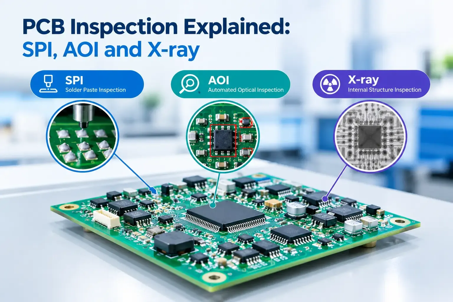
"Inspected" on a quote can mean anything from a person with a magnifying lamp to three different automated systems. Each method sees different things, and knowing what each one catches helps you ask the right questions of any assembly partner.
Solder paste inspection (SPI)
Where: right after the stencil printer, before any component is placed.
What it checks: the volume, height, area and position of every solder paste deposit, measured in 3D.
Why it matters: a large share of soldering defects, including bridges, opens and insufficient joints, begin as a bad print. Catching them at SPI costs a wipe and a reprint. SPI data also shows trends, such as a stencil starting to clog, before they turn into defects.
Automated optical inspection (AOI)
Where: after reflow, sometimes also before reflow.
What it checks: cameras and lighting from several angles compare each board with what it should look like:
- component present or missing;
- correct part (by markings and size);
- polarity and rotation;
- position and skew;
- solder joint shape on visible joints: bridges, insufficient solder, lifted leads.
Why it matters: AOI checks every part on every board consistently, which no human inspector can do across a full shift. With an auto-reject conveyor, failing boards are diverted automatically for review.
Its blind spot: anything it cannot see. Balls under a BGA, the thermal pad under a QFN, or joints hidden beneath a connector body.
X-ray inspection (AXI)
Where: after reflow, usually on a sample or on specific boards rather than in line.
What it checks: X-rays pass through the board and components, so you can see:
- BGA balls: bridges, missing balls and, with angled or 3D X-ray, head-in-pillow defects;
- voids in joints and thermal pads;
- hidden joints under shields and connectors;
- barrel fill on through-hole joints.
Why it matters: for boards with BGAs or large bottom-terminated parts, X-ray is the only non-destructive way to confirm those joints. It is also used when setting up a new reflow profile, and after BGA rework.
How they compare
SPI | AOI | X-ray | |
|---|---|---|---|
Stage | After printing | After reflow | After reflow |
Sees | Paste deposits | Parts and visible joints | Hidden joints, voids |
Coverage | 100% of boards | 100% of boards | Sample or targeted |
Cost to fix what it finds | Lowest | Moderate | Higher |
Inspection is not testing
All three methods confirm the board was built as designed. None of them proves it works. A board can pass AOI with the wrong firmware or a faulty part inside a perfect package. That is the job of electrical testing: see ICT vs functional testing.
Questions to ask your EMS partner
- Is SPI 3D, and is it applied to every board?
- Is AOI used after reflow on every board, and what happens to a failed board?
- How are BGAs and other hidden joints verified?
- Do you keep inspection data that can be traced back to a batch?
Inspection at Polyfit
Polyfit's SMT line runs solder paste inspection and automated optical inspection with an auto-rejection conveyor, backed by visual inspection to IPC-A-610 and functional testing. Ask us about the inspection and test plan for your board.
Send us a part number, a drawing or just the application. Our engineers reply within one working day.
Request a quote