Design for Manufacturing (DFM): Getting Your PCB Ready for Production
A board that works on the bench is not always a board that builds well. These are the DFM issues that come up most often, and how to fix them before they cost you.
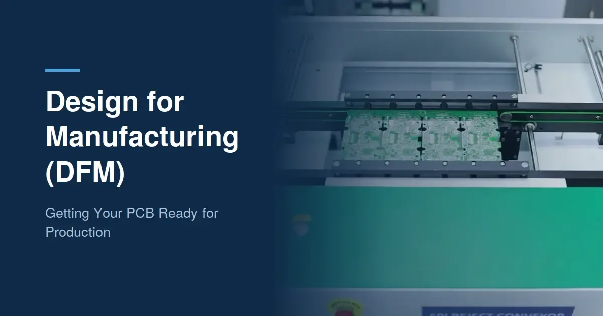
A prototype that works on the bench proves the circuit. It does not prove the board can be built 5,000 times with the same result. That second question is what design for manufacturing (DFM) is about, and it is where many projects lose weeks.
The good news is that most DFM problems are predictable. These are the ones that come up most often when a new design is quoted.
Footprints that do not match the part
The most common issue by far. A footprint drawn from a generic library, or for a similar part from a different manufacturer, can be off by enough to cause tombstoning on small passives or poor wetting on QFN thermal pads. Use the land pattern recommended in the component's datasheet, or one built to IPC-7352 (formerly IPC-7351), and check the parts with exposed pads especially carefully.
Components too close together
Placement machines and inspection cameras need room. So does a soldering iron if a part ever needs rework. Watch three things in particular:
- tall parts shadowing short ones, which hides joints from AOI cameras;
- SMT parts placed close to through-hole pins that will be wave soldered;
- large BGAs with no keep-out around them for rework.
No fiducials, or badly placed ones
Fiducials are the small copper targets the machines use to find the board's exact position. You want at least three per board, or per panel, placed asymmetrically so the board cannot be loaded the wrong way round. Fine-pitch parts benefit from local fiducials close by.
A panel nobody thought about
Small boards are built in panels, and the panel design affects yield. Add rails of about 5 mm for conveyor handling. Choose V-score or tab-routing to suit the board shape and any overhanging parts. Keep components clear of the break lines. A panel designed together with your assembler usually saves money.
Thermal problems in layout
A small pad tied straight into a large copper pour will not reach soldering temperature at the same time as its neighbour. The result is a tombstoned resistor or a cold joint. Thermal relief spokes on connections to planes solve most of this. On QFN thermal pads, split the paste opening into a grid (windowpane) to avoid the part floating on excess solder.
Missing test access
If you want in-circuit or flying-probe testing, nets need test points that a probe can reach. Even for functional testing, a few accessible power, ground and signal points make debugging far quicker. Decide on the test strategy during layout, not after the first batch fails. Our guide to ICT vs functional testing helps you choose.
A BOM that cannot be bought
DFM is not only about copper. A BOM with obsolete parts, single-source parts with 30-week lead times, or vague descriptions ("10k resistor") slows everything down. Give manufacturer part numbers, approve alternates where you can, and check lifecycle status before you freeze the design. We cover this in more depth in component sourcing.
Unclear polarity and assembly drawings
Diodes, electrolytic capacitors, LEDs and ICs need clear polarity marks on the silkscreen that match the pick-and-place data. An assembly drawing that shows anything unusual, such as parts fitted by hand, glue dots, special torque or a coating mask, removes guesswork.
A quick DFM checklist
Check | Why it matters |
|---|---|
Datasheet or IPC-7352 footprints | Prevents tombstoning, opens and poor wetting |
3+ asymmetric fiducials per board or panel | Accurate placement, no reversed loading |
Thermal relief on plane connections | Even heating in reflow |
Windowpane paste on large thermal pads | Stops parts floating, reduces voids |
Panel rails and break-away method agreed | Handling and depanelling without damage |
Test points on key nets | Faster test and debug |
MPNs and approved alternates in the BOM | Fewer sourcing delays |
Clear polarity marks | Fewer placement errors |
Make DFM part of the quote
The cheapest time to fix any of this is before the stencil is cut and the boards are fabricated. Polyfit's EMS division supports customers from design validation through assembly and testing, so raise manufacturability questions with your quote request. Request a quote.
From precision components to custom manufacturing, Polyfit delivers solutions tailored to your application and specifications.
Request a quote